In spite of its relatively simple structure, the AC PDP is a fascinating device that is rich in complex physical phenomena and device characteristics that can be exploited to improve product performance at reduced costs.
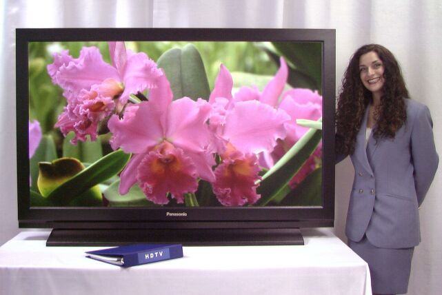
Plasma displays have achieved a high level of performance as demonstrated by the 60-inch diagonal prototype display shown in figure 1. This was for the first time demonstrated at the May 1999 SID International Symposium in San Jose and also at INFOCOMM 1999 in Orlando. The specifications for this display are shown in figure 2. The potential market for HDTV displays in home theaters is quite large and the plasma display has demonstrated that it can meet the very high quality requirements with an attractive form factor.
The major issue to be resolved before plasma displays will appear in most everyone's home is display cost. Costs are frequently broken down into two major areas: panel costs and circuit costs. While for today's manufacturing the panel costs more than the circuits, as manufacturing techniques advance, it is expected that the circuit costs will become dominant. The two problems of panel cost and circuit cost are closely coupled since there are many things that can be done to the panel that will make the circuit costs smaller and vice versa. For instance, if the panel can be manufactured with a more exact tolerance, then lower voltage address drivers can be used which translates to lower cost circuits. In another example, if the luminous efficiency of the panel can be increased then lower-cost, lower-power circuits can be used. Many times some seemingly small change in a circuit or waveform can have a major impact on the panel device characteristics which will make it accept wider manufacturing tolerances and thereby lower panel cost.
Plasma display device research can have a major impact on the reduction of both circuit costs and panel costs. We still have a great deal to learn about this intriguing device and much of it has remained unexplored. Powerful experimental and theoretical techniques are now being used to explain many challenging phenomena.
Fig. 1 Plasmaco's 60-inch Diagonal PDP for HDTV.
|
Pixel Matrix |
1366 x 768 |
|
Pixel Pitch |
0.972 x 0.972 |
|
Luminance |
450 cd/m2 |
|
Contrast Ratio (DR) |
500:1 |
|
No. of Colors |
16.7 Million |
|
Set Thickness |
133 mm |
Fig. 2 Specifications of 60-inch Diagonal PDP.
It is not possible to cover all of the many activities that are of significance in a short lecture. Instead, I will focus on an example from one device area to demonstrate the richness of physical phenomena and opportunities for device research.
I chose to experimentally evaluate the sustain gas discharge. While this is perhaps one of the most familiar aspects of the plasma display, it has many intriguing physical phenomena that need additional study.
One of the most powerful experimental tools for evaluating plasma display discharges is the image intensified CCD camera (ICCD). This tool records optical emissions in two-dimensional space and in time. Rather impressive results have been achieved at wavelength ranges from the near infrared to the vacuum ultraviolet [1,2,3]. Figure 3 shows an ICCD image of a single 1.08 mm by 1.08 mm RGB pixel measured on the current Panasonic 42 inch diagonal plasma display product. This is a 10 nanosecond shutter snap-shot of the near IR light near the peak of the sustain discharge. The very interesting mushroom shaped discharge pattern can tell us a great deal about the discharge characteristics.
The figure 3 device has the usual color PDP structure having a front plate with wide tin oxide electrodes, which are reinforced with highly conductive opaque electrodes, which are seen in figure 3 as horizontal dark bars above and below the discharge light. The back plate has the usual data electrodes, phosphors and also the barrier ribs, which are seen in figure 3 as the vertical dark bars that separate the discharges. In this device a high color temperature is achieved by making the blue phosphor channel the widest and the red phosphor channel the narrowest.
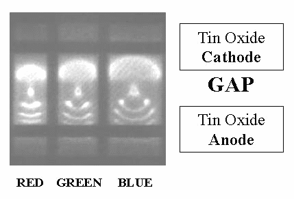
Fig. 3 IR light from RGB pixel near discharge peak
The image of figure 3 shows an anomalous interference pattern that produces lines at 45 degrees that are considered instrumentation error and should be ignored.
The near IR light measured in figure 3 comes from the excited xenon atoms and conveniently approximates the areas where vacuum UV light is generated. Of course the vacuum UV light is used to excite the phosphors to generate the display's visible light.
It is interesting that IR light (and therefore UV light) is generated along both the cathode and the anode. It is clear from figure 3 that the mechanisms for light generation are quite different between the cathode and the anode. The anode has the fascinating curved structures called striations, whereas the cathode has the more continuous mushroom top shaped area with the rounded top. The region between the cathode and the anode, called the gap, has a very bright small region that is at the very center of each sub-pixel, which corresponds to the stem of the mushroom.
Figure 4 shows the orange light from neon for the exact same conditions as in figure 3. There is a remarkable difference in the two light patterns. The orange neon light appears only on the cathode and is positioned along the top surface of the IR xenon light mushroom seen in figure 3.
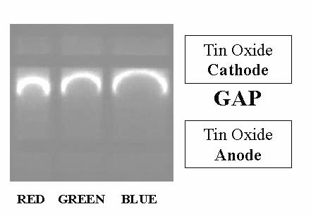
Fig. 4 Orange light for same conditions as figure 3
The reason for this difference of IR and orange light is predominantly due to the different conditions required to excite xenon and neon. To generate the IR light the xenon atom must be excited to at least 9.82 electron volts. To generate the orange light the neon atom must be excited to the much higher level of 18.96 electron volts.
The gas mixture used in this device is neon plus 5% xenon. When electrons flow through this mixture the collision cross-section for the xenon atoms is much larger than that for the neon atoms, even though there are 20 times as many neon atoms. This is because the outer xenon electrons are much more loosely bound due to the strong shielding of the many inner shell electrons. The cross-section difference means that as free electrons gain energy from the electric field they are more likely to excite the larger cross-section xenon atoms, which requires lower energy. The neon atoms only get excited at the regions where there are very high electric fields. In these regions a small number of electrons will acquire the high kinetic energies necessary to excite the neon atom. This means that the neon light is a convenient indicator of the very high field regions of the discharge [3].
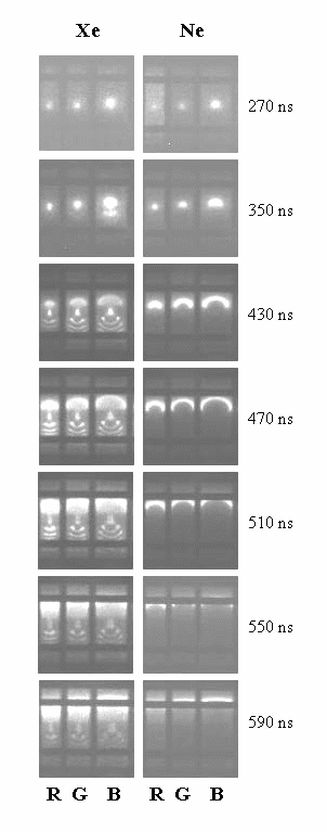 Fig. 5 Selected frames from discharge light movie |
Figures 3 and 4 show the light for just one instant (10 ns) of the
sustain discharge. Considerably more can be learned about the discharge by
taking a time-delayed sequence or movie of the discharge process. Figure 5
shows selected frames from a movie of the sustain discharge. The left-hand
column frames show the IR xenon light similar to figure 3 and the right
hand column frames show the orange neon light like figure 4. Each of these
frames is for a 10 ns exposure. The times are specified with zero time at
the beginning of a 400 nanosecond rise sustain pulse. The brightness and
contrast of each frame was individually adjusted to show the greatest
amount of information for a given frame. Figure 5 does not allow the
comparison of light intensities for different frames. |
It is clear from figure 5 that the top of the mushroom is a cathode wave that is initiated near the center of the sub-pixel at time t=350 ns and propagates along the cathode until it reaches the cathode. This wave propagates at the velocity of approximately 1000 m/s.
There is a much faster wave that propagates along the anode. It is not visible in figure 5 but it moves quickly from the center of the sub-pixel to the bottom edge of the anode between the frames for t=350 ns and t=430 ns. The velocity of the anode wave is approximately 4000 m/s.
The phenomena of slow cathode waves and much faster anode waves with striations were observed many years ago in monochrome panels with the monochrome two-substrate structure [4]. The velocity of the two waves is considerably different because of the mobility difference of electrons and ions. The highly mobile electrons can easily move out of the plasma in the anode region and thereby allow the anode wave to have a high velocity. Alternatively, the low mobility ions control the growth of the cathode wave making it much slower. A quantitative theoretical explanation of these waves that predicts the wave velocity is an opportunity for some good theoretical work.
Striations have been observed in the positive columns of many gas discharges and so it is not so unusual to find them in the anode region of the plasma display. Striations indicate periodic electric potential variations that are due to the accumulation of space charge. As one moves along the anode each striation indicates a step in potential of approximately 10 volts. This corresponds roughly to the xenon ionization and excitation potentials.
The beautiful curved pattern of the striations is a convenient indication of the equipotential lines along the anode. Similarly, the leading edge of the cathode wave indicates an equipotential line along the cathode. It is quite interesting that the anode and the cathode equipotential lines are nearly concentric with the center of curvature near the stem of the mushroom. This is because the stem is where the discharge was initiated as shown in the top row of figure 5 at t=270 ns. Like a pebble dropped in water, the waves radiate out from the initial disturbance. In AC plasma displays, the anode wave propagates at a much higher velocity that the cathode wave.
It is helpful to develop a simple circuit model for the sustain discharge shown in these figures. At the peak of the discharge shown in figures 3 and 4, the model of figure 6 is appropriate. This figure also shows the qualitative features of the front plate dielectric potential measured along the vertical sub-pixel centerline. The distributed dielectric of the front plate is modeled as a number of lumped capacitors.
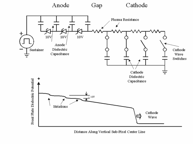
Fig. 6 Circuit model for discharge peak.
On the anode side, the striations are modeled as 10-volt avalanche diodes. There is one diode for each striation. The energy loss across each avalanche diode represents the average energy lost in ionizing and exciting the xenon atoms.
On the cathode side, the cathode wave is modeled as a number of switches. As the cathode wave moves along the cathode dielectric, the switches close one at a time and connect the cathode dielectric capacitor to the rest of the conductive plasma.
The plasma in the cathode region and in the gap is modeled as a resistance. Like the striations, the energy lost across this resistance goes to the ionization and excitation of xenon atoms. Unlike the striations there is no spatially periodic order to this loss process.
The model of figure 6 shows that the current that flows through the discharge is primarily limited by the rate at which the cathode wave switches close. This has very important consequences for the plasma display circuits. The sustain circuit and the panel electrodes always have some parasitic inductance and resistance which will reduce the voltage applied to the pixels during the sustain discharge. If the sustain discharge current is very high then an undesirably large voltage will be dropped across the parasitic resistance. If the rate of rise of the discharge current is too large, then the parasitic inductance will drop too much voltage. Fortunately, the slow movement of the cathode wave significantly limits the peak current and also the rate of rise of current. This allows large panels to be made with manageable pulsed discharge currents.
The dielectric potential diagram of figure 6 shows a very large potential drop across the front of the cathode wave. The regions to the left of the front are at a much more positive potential that the regions to the right. Looking at figures 3 and 4, the dielectric above the top of the mushroom has a much lower potential than the dielectric within the mushroom. This potential drop is very common in gas discharges and is known as the cathode fall. It usually has a magnitude on the order of 100 volts, however this author is not aware of any measurements of it for AC plasma displays.
This cathode fall is of great significance for plasma displays. The very high potential drop across the cathode fall allows the neon atoms to be excited as in figure 4. However this high field region is very inefficient in exciting xenon atoms that supply the desirable vacuum UV light. Unfortunately, the cathode fall is efficient at generating xenon ions with high kinetic energies that can sputter the MgO surface. It is possible that a small population of xenon ions can gain the full potential drop of the cathode fall without making an energy reducing collision and then deposit that large energy to the MgO surface where sputtering damage will occur. SEM analysis of sputter eroded MgO from plasma displays shows patterns that conform exactly to the path swept by the cathode wave.
Figure 3 shows a hole in the center of the stem of the mushroom. This hole is not observed in earlier frames and develops as the discharge progresses. This hole is believed to be due to self absorption of the IR light by the gas. If a sufficient density of xenon metastable atoms or imprisioned resonant atoms exists, then the IR photons can be absorbed by these excited atoms. The gas actually looks dark at the measured IR wavelengths. This absorption has been measured in space and time [5], and conveniently indicates regions of intense excited xenon atom density.
One area of significant activity worthy of mention is the excellent gas discharge simulations developed by a number of workers [6,7]. Many of the effects shown in figures 3, 4 and 5 are explained by these simulations. One notable exception is the modeling of the striations which may require a time consuming multi-dimensional Boltzmann algorithm.
It is clear that the rather familiar AC plasma display sustain discharge is not so simple. We are just beginning to understand the important elements of this discharge and how we can make better plasma displays by adjusting certain critical parameters. The opportunities for continued research on this device are many. One major area of study that is currently commanding a great deal of resources but understandably little public information is the increase in luminous efficiency of the sustain discharge. A clear understanding of the detailed dynamics of this discharge will greatly aid this pursuit of higher efficiencies.
[1] M. Sawa, T. Tsutsumi, K. Yoshida and H. Uchiike,"Characteristics of Surface-Discharge ac Plasma Displays by Direct Observation of Vaccum Ultraviolet Rays," 1999 SID Int. Symp., pp. 284-287.
[2] C. Yoon, et al,"Spatio-Temporal Variation of VUV and IR Emission from Surface Discharge Type ACPDP Cell," 1999 SID Int. Symp., pp. 272-275.
[3] T. Shiga, K. Igarashi, and S. Mikoshiba,"Visualization of a PDP Discharge Growth and an Interpretation of the Growth Mechanism," 1998 Int. Disp. Workshop, pp.487-490.
[4] L. Weber and C. Steiner,"Domains in AC Plasma AND Gates," 1984 SID Int. Symp., pp. 180-183.
[5] A. Okigawa, T. Yoshida, and K. Tori,"Diagnosis of ACPDP Micro-Cell Dsicharges by Space and Time-Resolved Laser Absorption Spectroscopy," 1999 SID Int. Symp., pp.276-279.
[6] J. Boeuf, T. Callegari, C. Punset, and R. Ganter,"Modeling as a Tool for Plasma Display Cell Optimization," Asia Display'98 Workshop, pp. 209-220.
[7] P. Drallos, V. Khudik and V Nagorny,"3-D Simulations of a Single-Substrate ACPDP Cell with Barrier Ribs," 1998 SID Int. Symp., pp. 632-635.